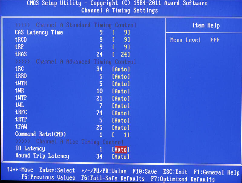
Let's switch to Gigabyte high-end motherboard for Core i7 2000 series CPU.
Vcore
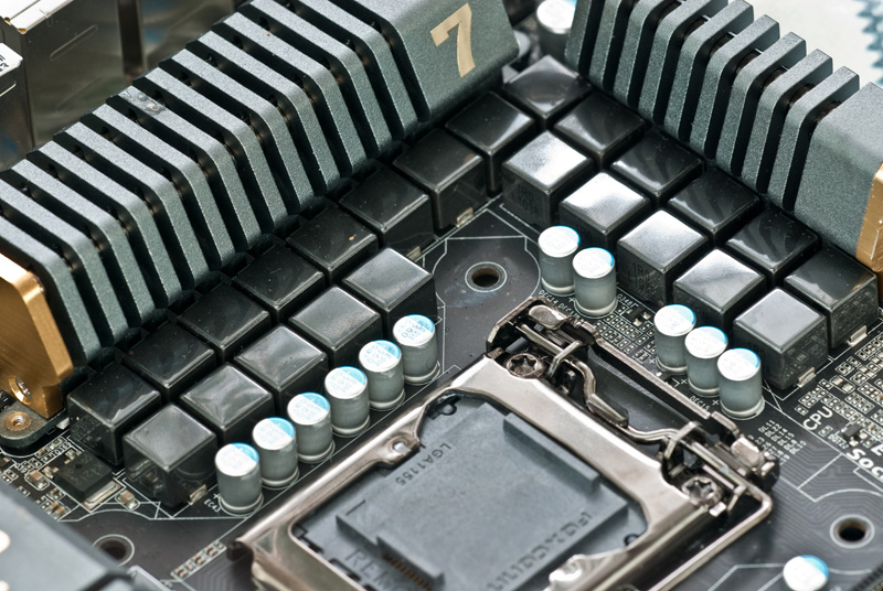
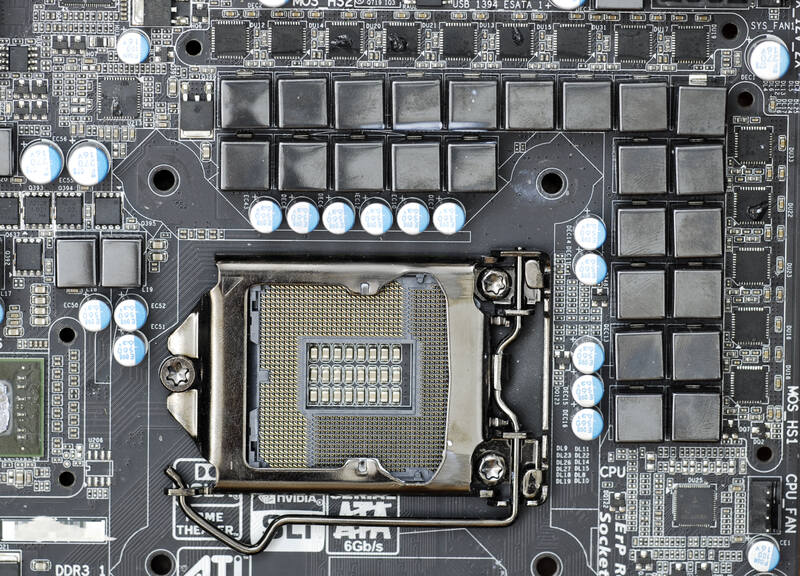
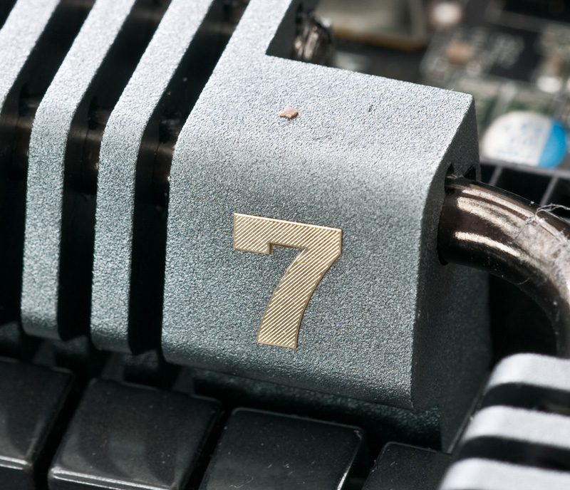
Main VRM covered under nice-looking heatsink with "7" labeling. UD5 have blue decoration and "5"

. I like the design of new P67A boards, they look much more high-end than previous cyan boards.
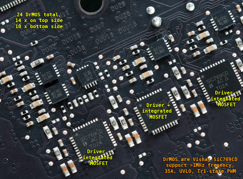
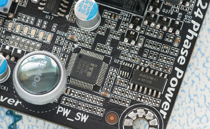
Lots of inductor coils. Lots. 24 of them. Looks great, but none of consumer PWM power controller support 24 phase operation directly. Most advanced devices, like Volterra 1185MF able to control 10 phases. So we have here phase split, when one PWM channel used to control more than one physical buck circuitry. By simple calculation we get here 6-channel PWM topology.
6 real phases * 2 (double) * 2 more = needed "24" phase. But if you add something at one side, it's always a sacrifice in something other. Let me show schematic view, where topology will look like this:
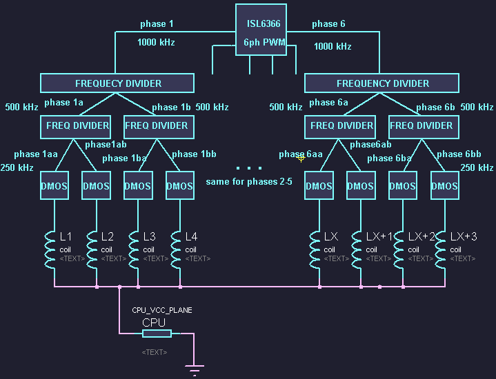
There is no technical need to make such complex system. Having more phases does not mean that CPU will get more power. Multi-phase systems made because it's simpler to spread big high-current load to separate nodes, so each node converts only part of whole power needed. But having too much nodes may lead to excessive noise and voltage deviation, because it's more difficult to control many nodes with high-speed PWM channels. As in general it's better to have some golden middle solution.
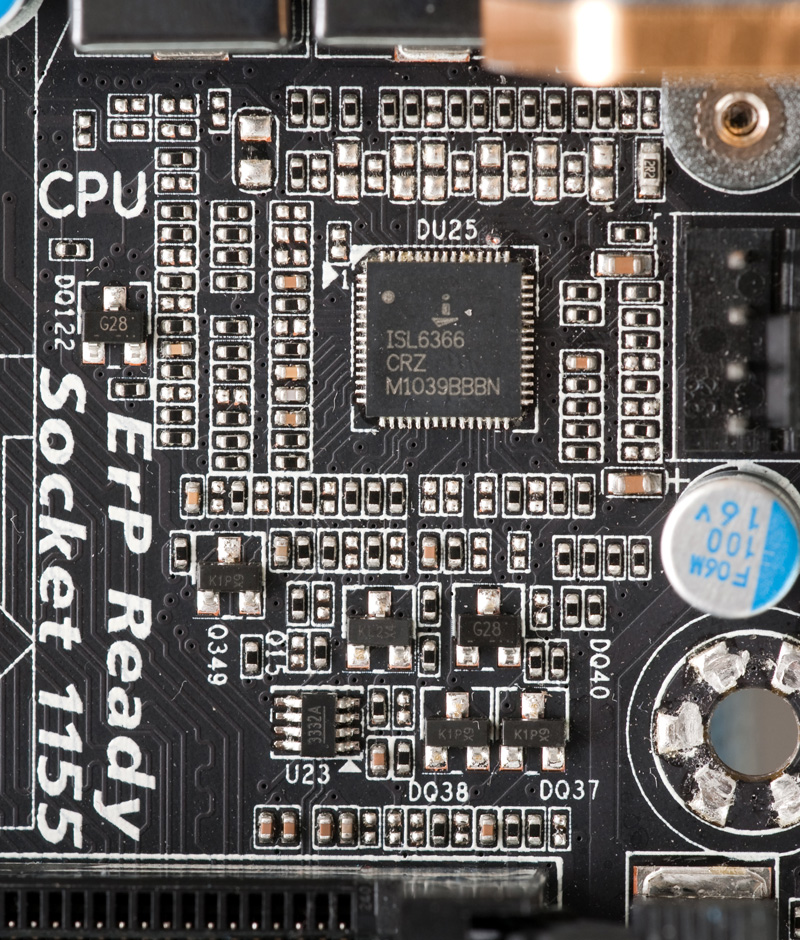
So Vcore for CPU is controlled by
Intersil ISL6366 chip. PWM signals go to frequency divider (small chips with 5 pins each side, labeled 617C FLBK). Frequency divider takes input signal, in our case 1000kHz from ISL6366 PWM channel and make two output signals with half frequency (inverted+normal). Then these two outputs are divided again by two more frequency dividers, whose outputs are finally drive DMOS chips at 1/4th frequency of original input PWM signal, 250kHz in out case. Each DMOS chip is a hybrid IC with two MOSFETs and their driver. So each PWM channel from ISL6366 flow thru three dividers to reach MOSFET gates. Frequency is always 1/4 of PWM phase. So with such unit it's impossible to archieve fast rate 1MHz, as on "true" multi-phase PWM topology. DMOSes used are Vishay SiC769CD, each rated to 35A.
So looks like customer pays his dollars for lots of inductors, power chips, passives just to have nice looking thing, but not for actual performance. We will check if this statement true or false during practical test.
Quite crazy to make such a complex topology, if you ask me

.
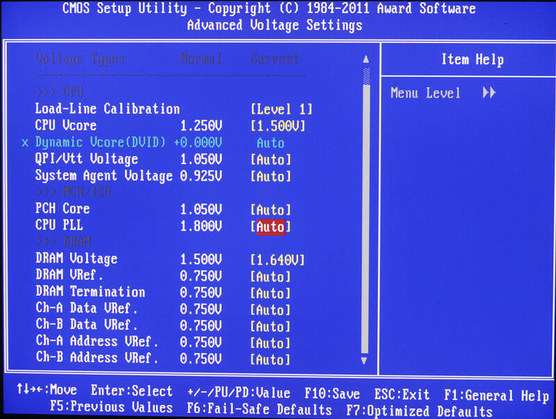
Voltage adjustable from BIOS, in range 0.750 to 1.700V, with 5mV step. 1.7V may be too low for real extreme guys.
CPU PLL power
CPU PLL voltage is adjustable in range 1.52 to 2.52V, with 20mV step.
System agent power
SA Voltage is adjustable, in range 0.655 to 1.305V, with 10mV step.
DRAM power
ISL6322G does work for powering memory sticks. It have dual phases to convert power, each with
Renesas µPA2726UT1A FETs. Nothing interesting else to say about, this PWM chip is already known by other Gigabyte boards and high-end videocards.
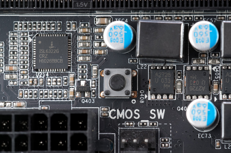
This voltage is adjustable under name DRAM Voltage, in range 0.9 to 2.6V, with 20mV step.
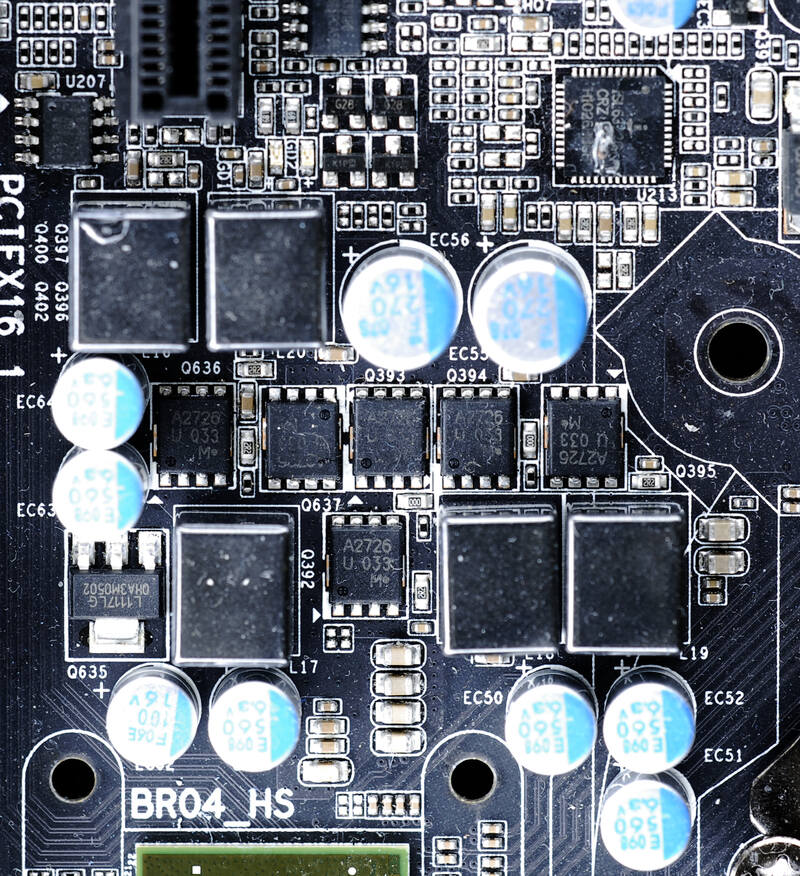
For VIO power UD7 uses similar ISL6322 paired with two phases. Mosfets in each phase are
Renesas µPA2726UT1A. Each FET can push 20A.
Input capacitance is 2 x 270uF 16V, output is decoupled by three 560uF, total 1680uF.
In Gigabyte's BIOS this voltage is adjustable under name QPI/Vtt Voltage, in range 0.8 to 1.7V, with 20mV step.
Also NF200 power placed nearby, controlled by simple 8-pin PWM Controller ISL6545 and single phase with pair of same µPA2726UT1A.
Output decoupled by three 560uF LowESR caps.
PCH power is maintained by simple PWM controller, maybe ISL6545, hidden under CMOS battery holder, with two Renesas FETs and few 560uF caps. Had no need to desolder battery holder to read PWM marking.
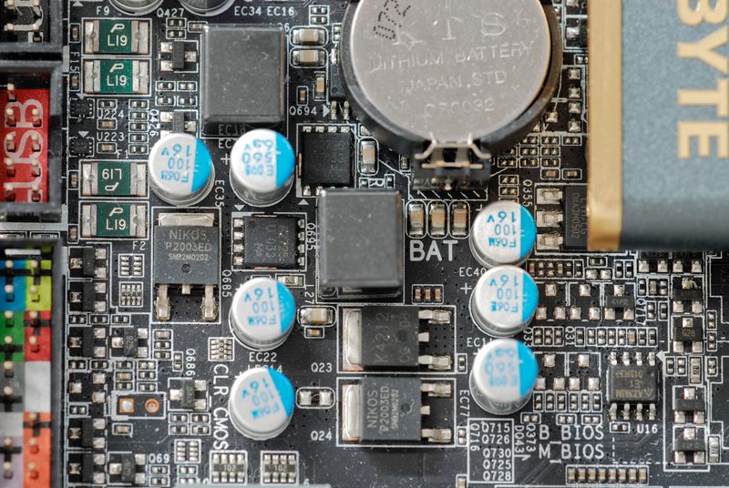
In BIOS this voltage is adjustable under name PCH Core Voltage, in range 0.84 to 1.94V, with 20mV step.
Features
I think most reviewers already covered widely known things about new platforms, so just stop by on most interesting things.
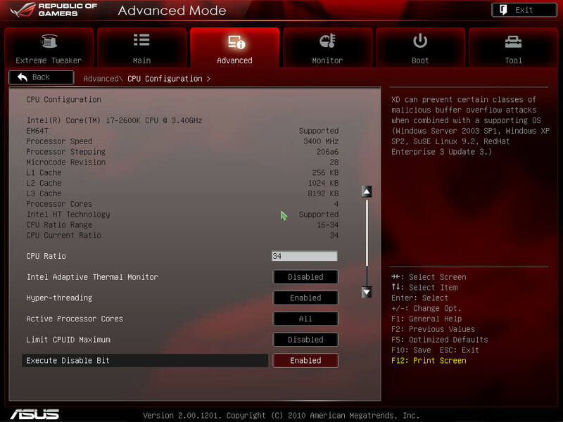
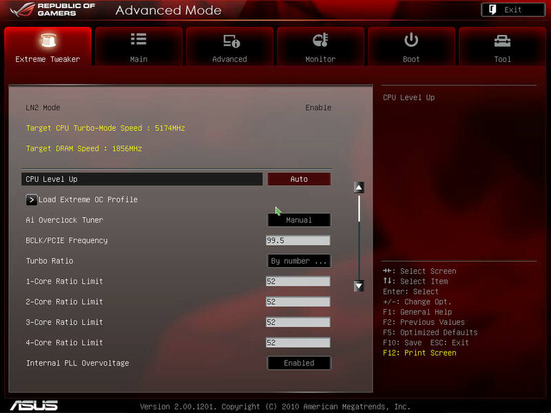
ASUS Maximus IV Extreme
Board have PCI-Express Gen2 differential buffer
IDT 9D403DGLF to drive down-stream PCI-Express cards.
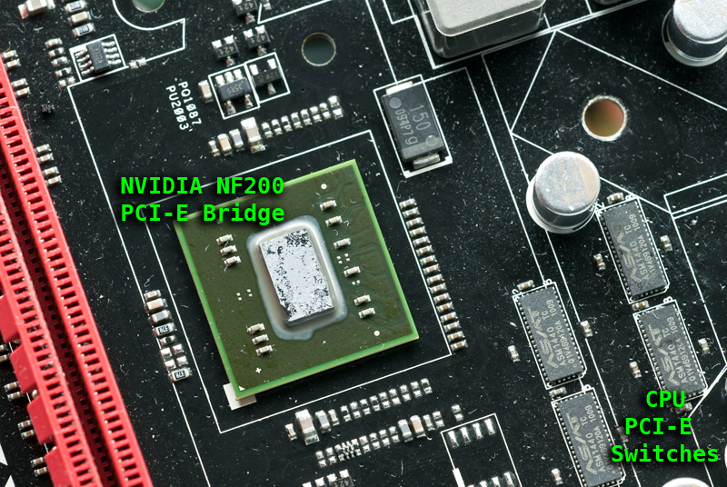
Well known NVIDIA NF200/BR04 bridge used to add two more PCI-E slots to Sandy Bridge platform.
NF200 and CPU VRM circuitry cooled by single heatsink assembly. Cooling solution is low-profile and aligned well.
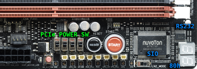
Overclockers like buttons for power and reset onboard. Also voltage check points are useful during extreme testing and for controls. Just a note here - fine-pitch connectors for monitoring cables is not a solution for most of guys, MSI ones for regular DMM probe are much better in term of usability.
LN2_Mode switch will allow easier overclocks under subzero by idea, but seems doesn't work actually on Sandy Bridge CPU's.
There also cool PCI-Express disable switches, to power down PCI-E card installed in selected slot. We saw similar idea
on Classified high-end boards. Should be nice feature for those who push hard 2-way/3-way SLI/CF rigs. GO_BUTTON loads profile from BIOS on-fly.
Some iROG controller which does something useful for enthusiasts. It has NOR flash chip near to store some data, maybe OC profiles etc.
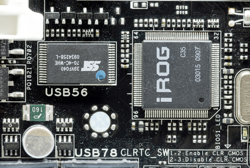
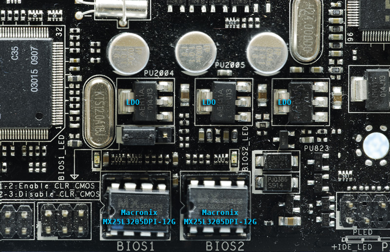
Maximus equipped with two BIOS SPI Flash chips. I like also LED which show currently selected and used BIOS. Visible and usable.
Overall platform view with cooling installed:
Gigabyte P67A-UD7
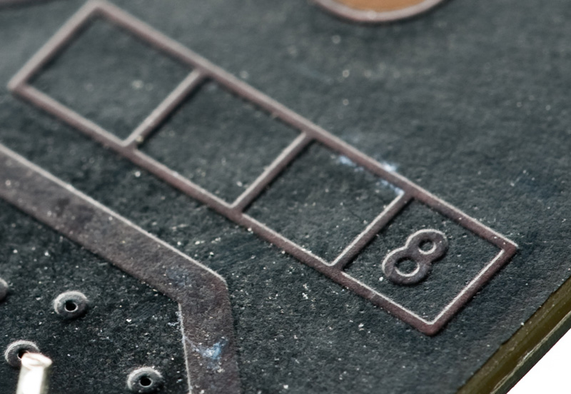
Marking with 8 layers of copper stack up.
Passive heatsink have nice look and does its job just ok.

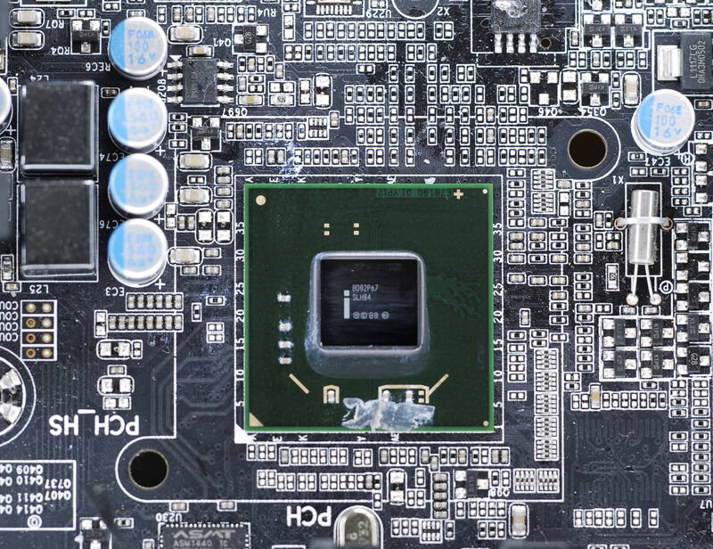
PCH area crowded by lots of 0402 resistors, capacitors and discretes. PCH chip does not have any visible from top "bridges" or straps to solder on
.
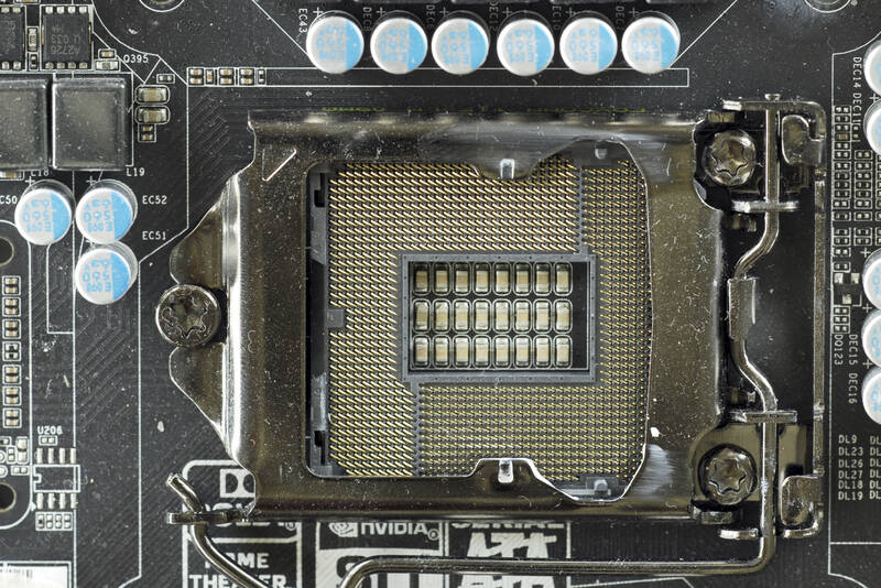
Same as ASUS board, here is used Foxconn socket. Time will show if socket burns affect 1155 platform.
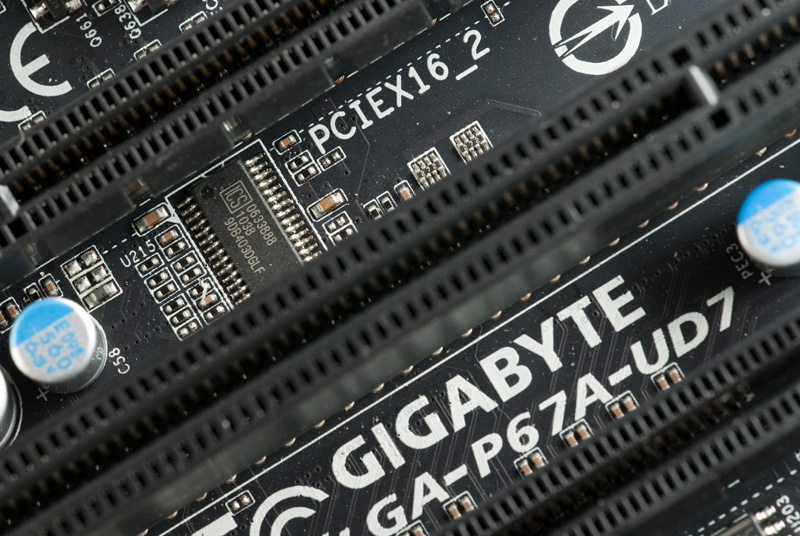
UD7 have two PCI-Express Gen2 differential buffers
IDT 9D403DGLF which take source clock and drive to PCI-Express down-stream devices.
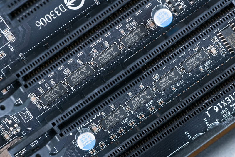
PCI-Express slots use NF200 even if not connected to, so it's always heating here. Slots locks are comfortable and easy to use, much better that ASUS big ones.
Board also have power button, reset button and clear cmos button, but no hardware monitoring points.
I guess UD9 should be black-styled
Here we have UD7 symbol.
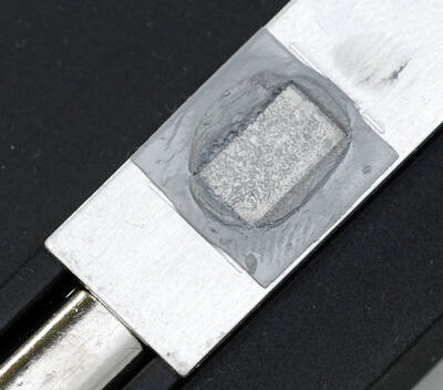
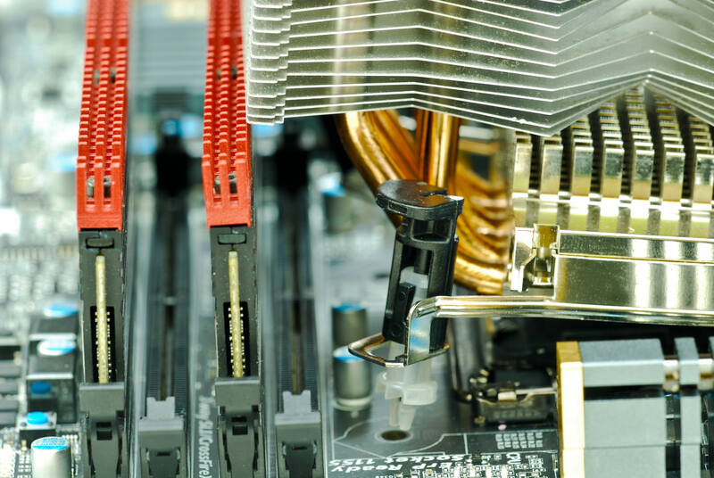
Now remove cooling solution and check...
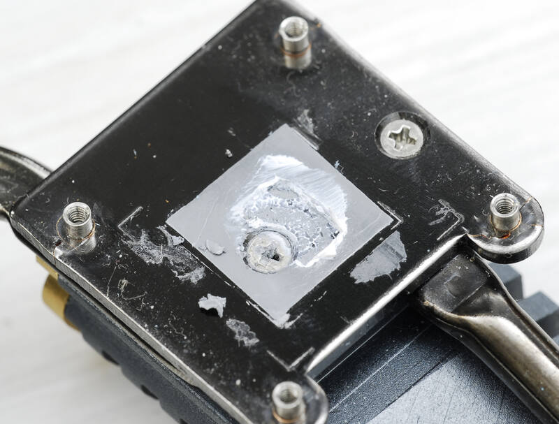
Contact area of motherboard heatsink is not as good as expected to be, mount screw placed just above NF200 die. First time I saw such a "solution" on high-end motherboard

Software and firmware
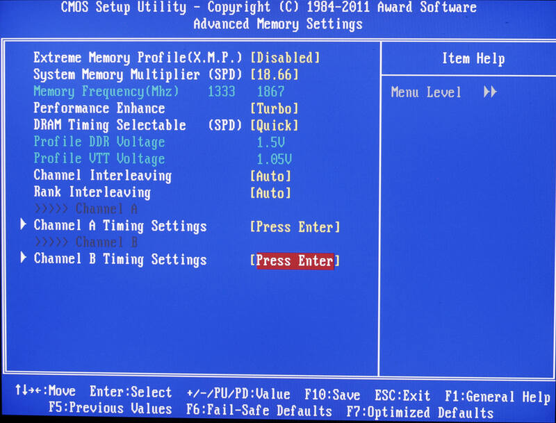
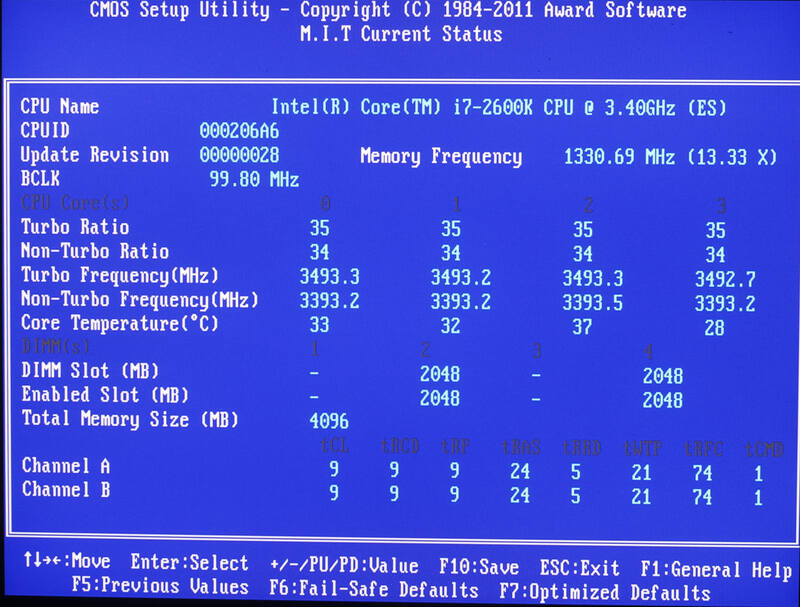
BIOS shots of Gigabyte and ASUS boards. ASUS used UEFI for their latest P67 boards, while GBT still use legacy well-learnt Award.
UD7:
P67A-UD7 can be controlled under proprietary EasyTune6 tool, which is as usual is not easy at all in real-life overclocking. It does not work well with all bios versions, have overwhelmed design, but lack of necessary functionality, like system voltage monitoring and controls. Controls are laggy. Pity, such issues are common for "uber-super-overclocking tools" shipped with modern motherboards. Why not to create really simple and working tool, like SetFSB/CPU-Z/Rivatuner with simple interface w/o heavy graphics, just to do the job needed, fast and easy?..
M4E:
Maximus have similar overclocking tool too, but this one not as laggy, just need better usability, for example to have all settings on one screen section, not that countless folders in folders in submenus with only two-three settings in each
.
Benchmarking
Tier 1 : The Beginning
First to do - assemble test system and check if everything run smoothly and stable.
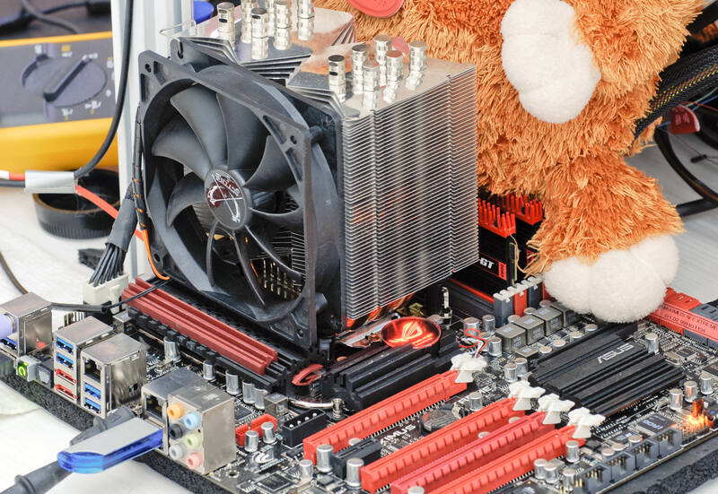
Start from CPU cooler install.
Clearance check for not the biggest cooling solution - Scythe Yasya in horizontal position.
On both boards cooler block nearest to CPU socket memory slot for any module with high heatsinks.
Even Dominator GT installed to second slot from socket with their accurate heatsinks was very close to touching
CPU cooler on ASUS board, and failed to fit with Gigabyte P67A-UD7.
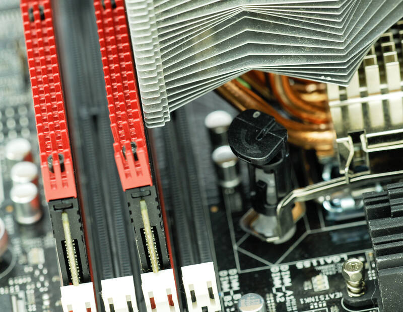
Almost touched.
Fail to fit.
Of course it's not only motherboard design issue, but rather memory vendor stuff. Nice fancy heatsinks on
DDR3 stick are not for cooling, but for cool looking. Power output is so low for modern memory that it's not an issue
at all. And most extreme guys who cool memory to subzero are anyway don't care about awesomeness of stock
heatsinks on memory.
After assemble both boards boot and fully functional. Gigabyte P67A-UD7 had some issues with
Gigabyte PSU, I tried to use Odin GT 550W for some preliminary use, but board didn't even power on. Instant
shutdown when I press Power button. System doesn't power on even with everything disconnected.
Same PSU works okay with rest of my rigs, including Gigabyte P965-DQ6, ASUS P6T6, Maximus IV Extreme.
Maybe it's just exact PSU/mobo combo issue, but it was fun to have GBT PSU not working with GBT board.
2nd test - monitoring accuracy for voltages
Interesting part here. I will check all the voltages with Fluke 87V DMM and compare that to BIOS/Software
monitoring readout. For both boards I've set next settings from BIOS setup:
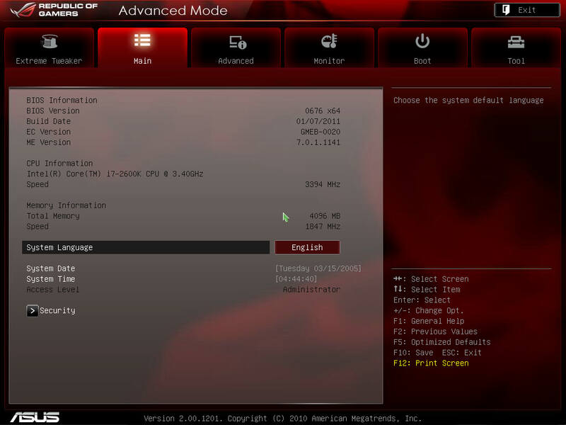
ASUS M4E - BIOS version 0676 x64 from 01/07/2011, EC: GMEB-0020, ME: 7.0.1.1141
Quote:
BCLK/PCIE Frequency: 100.3
Turbo Ratio: 52
Internal PLL Overvoltage: EN
Memory Frequency: DDR3-1857MHz
EPU: Disabled
CPU Manual Voltage: 1.500
DRAM Voltage: 1.65V
Rest voltages left Auto
Spread Spectrum: DIS
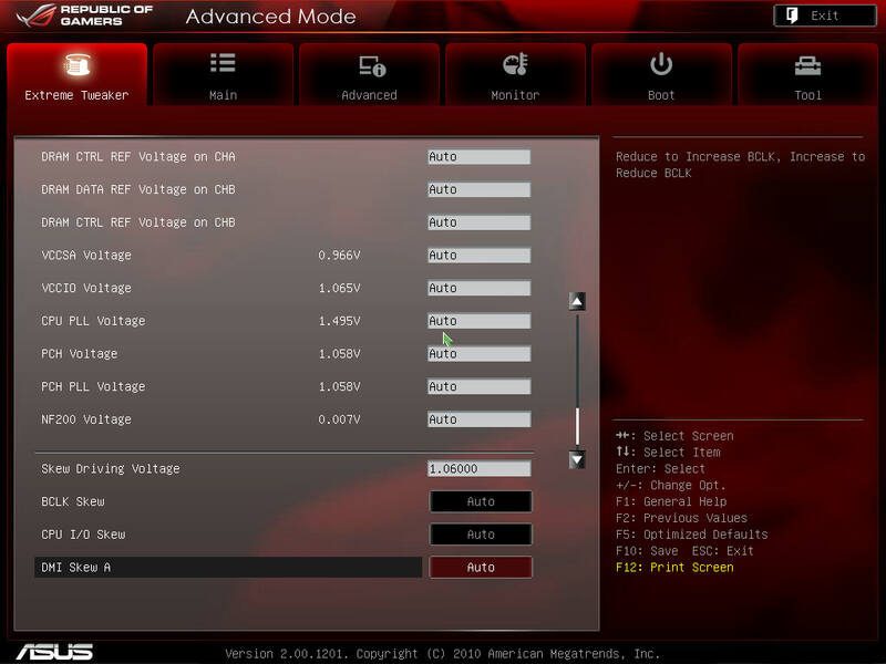
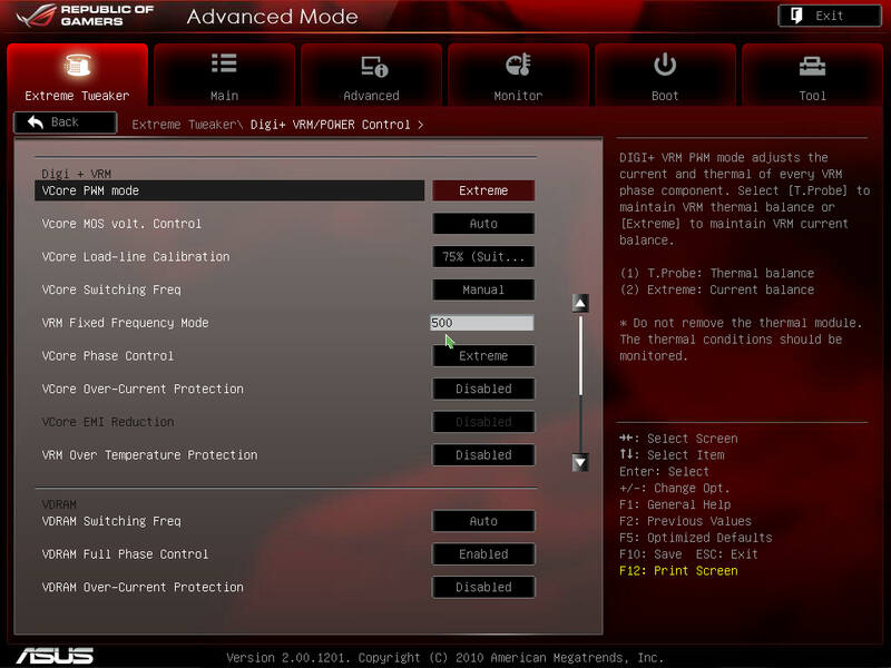
Digi+ VRM Control:
Vcore PWM mode: Extreme
Vcore MOS volt. Control: Auto
Vcore LLC: 75%
Vcore Freq: Manual, 500kHz
Vcore Phase control: Extreme
Vcore OCP: DIS
VRM OTP: DIS
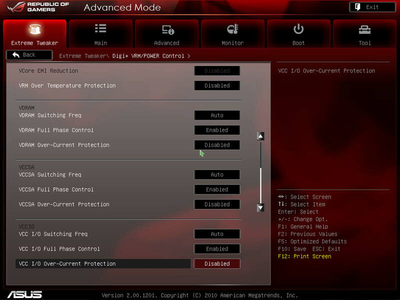
Rest convertor settings left Auto, Full Phase Control everywhere set EN
CPU settings:
Ratio: 34
Intel TM: DIS
HT: EN
Active cores: ALL
SpeedStep Tech: EN
Turbo: EN
C1E, C3 Report, C6 Report: DIS
All onboard devices disabled.
|
Gigabyte UD7 - BIOS version F7a from 01/07/2011
Quote:
BCLK/DMI/PCIE Frequency: 100.3 MHz
Turbo Ratio: 52
Internal PLL Overvoltage: EN
Memory Frequency (SPD multiplier): DDR3-1857MHz (16.00)
EPU: Disabled
CPU Manual Voltage: 1.500
DRAM Voltage: 1.65V
Rest voltages left Auto
Spread Spectrum: DIS
Digi+ VRM Control:
Vcore PWM mode: Extreme
Vcore MOS volt. Control: Auto
Vcore LLC: Level 1
Vcore Freq: Manual, 500kHz
Vcore Phase control: Extreme
Vcore OCP: DIS
VRM OTP: DIS
Rest convertor settings left Auto, Full Phase Control everywhere set EN
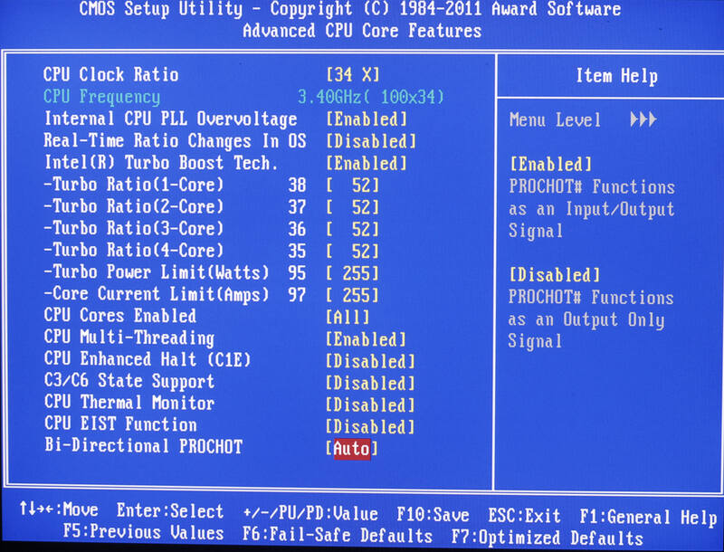
CPU settings:
Ratio: 34
Intel TM: DIS
Turbo Power Limit (Watts) - 255
Core Current Limit (Amps) - 255
HT: EN
EIST: DIS
Active cores: ALL
SpeedStep Tech: EN
Turbo: EN
C1E, C3 Report, C6 Report: DIS
All onboard devices disabled.
|
CPU Vcore monitoring
Min, max and average value during idle and one cycle of SPI,wPrime,Vantage CPU and Aquamark tests according to meter.
ASUS board
LLC 75%
Average voltage photo, 1.5065V
Maximum voltage photo, 1.5083V
Minimum voltage photo, 1.5029V
Less than 10mV delta from min to max. Nice results and precise setting.
LLC 100%
Average voltage photo, 1.5661V
Maximum voltage photo, 1.5761V
Minimum voltage photo, 1.5606V
So max delta is about 15mV, and total voltage level is steady 60mV above BIOS 1.500 setting.
Gigabyte board
LLC Level 2
Average voltage photo, 1.5608V
Maximum voltage photo, 1.5988V
Minimum voltage photo, 1.5523V
46.5mV delta from low load to high load. Average level is 56mV above BIOS settings, topping at almost 1.6V.
LLC Level 1
Average voltage photo, 1.4982V
Maximum voltage photo, 1.5125V
Minimum voltage photo, 1.4749V
37mV delta, average level is quite near 1.500 V setting in BIOS.
So quite stable operation under heavy transitions from idle to 8-threaded wPrime/Vantage, I must admit.